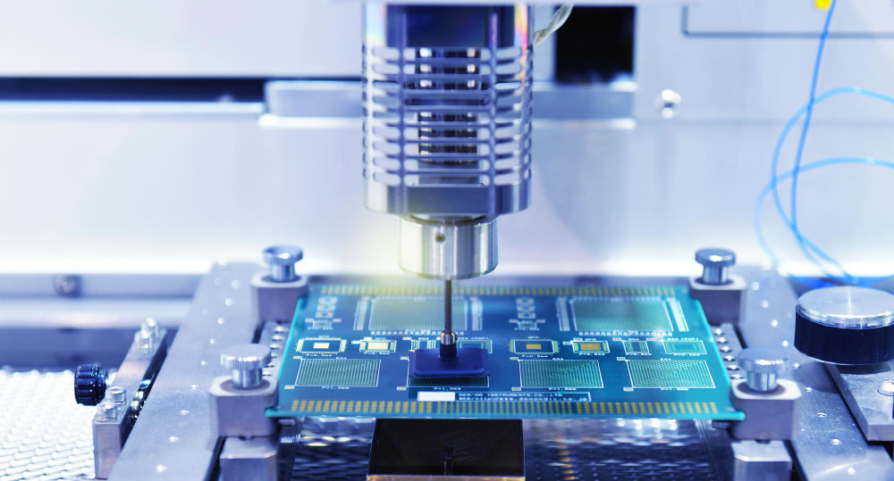
Devroop Dhar, CEO and Co-founder, Primus Partners, shares his view on India’s expanding capabilities in advanced semiconductor packaging, emphasizing the growing importance of Wafer-Level Packaging (WLP). He highlights that WLP allows for shorter internal chip connections, leading to faster speeds and greater power efficiency—critical for miniaturized devices like smartphones, wearables, and IoT solutions. As the semiconductor industry shifts focus from transistor scaling to packaging innovation, WLP is becoming central to next-generation chip production.
He further explains that WLP sits higher in the semiconductor value chain than traditional packaging and demands investments in cleanroom environments, precision tooling, and specialised engineering talent. With India greenlighting the HCL-Foxconn WLP initiative, this marks a serious move toward domestic advanced packaging infrastructure.